Why next generation TVs need perovskites
Link to this article in Chinese 电视为何需要钙钛矿
In a previous blog article, we explained how in-pixel colour conversion is driving innovation in TV displays whether based on LCD, OLED or µLED. Since then, we have seen increasing momentum and interest in the in-pixel approach both behind the scenes and in public, for example with the positive buzz around Samsung’s “QD-Display” at CES2022. In this follow-up article, we summarise why perovskites are the best material option for in-pixel colour conversion in TVs.
Colour conversion at the pixel level
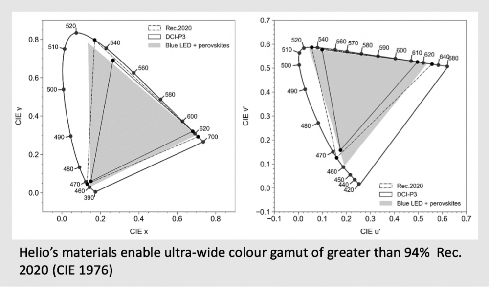
Colour conversion is the process of converting incident light into a single very pure colour using photoluminescent materials. Typically, when done at the pixel level, blue light from a backlight, OLED layer or µLED is converted to green in the green sub-pixels and red in the red sub-pixels. This pure red and green light enables very high colour gamuts and power efficiency gains of up to 70% to by converting light rather than filtering it.
To deliver on its promise of new levels of performance and efficiency in displays, in-pixel colour conversion will require a compatible set of patternable red and green photoluminescent materials that can be easily processed by the display industry.
The uniqueness of perovskites
It is fundamental to in-pixel colour conversion that the conversion layer can be patterned at high resolution leading to the requirement for optical layers that are as thin as possible to increase patterning accuracy. Layer thickness also sets limits on minimum pixel size because of the mechanical and optical design issues that arise with pixels that have tall and thin aspect ratios. For inkjet deposition, thinner layers reduce deposition time leading to capital and operating cost savings.
Perovskites are fundamentally different to quantum dots as their emission wavelength is primarily defined by their chemical composition and not by quantum confinement. Perovskites have higher optical density than quantum dots enabling significantly thinner conversion layers. Helio is developing red and green materials that achieve an optical density to blue light of 2 to 3 (that is 99% to 99.9% absorption) in a layer thickness of a few microns.
In addition to higher absorption, perovskites have the advantage over quantum dots in efficiency, colour purity and manufacturing. Phosphors can have good efficiency and purity at least for red, but their slow response time and low optical absorption is a severe limitation for in-pixel applications.
We are often asked whether the optical absorption advantage of perovskites over quantum dots is fundamental. The answer is yes because perovskites have intrinsically very high absorption and, unlike quantum dots, they do not require core-shell structures which take up volume whilst not absorbing blue light.
The high optical density of perovskites offers a further opportunity for simplification in the display stack by making it possible to remove the colour filter completely and still achieve a high colour gamut.
Deposition and patterning
Helio is developing compatible red and green core materials that can be formulated into a range of final product forms. We expect that the two most important product forms will be jettable inks and photoresists (similar to colour filter photoresists).
Photoresists are of particular interest because they can be used in established and mature manufacturing processes and have the potential to support smaller feature sizes than inkjet. In Summer 2021, Helio demonstrated the first perovskite proof of concept photoresists for both red and green.
Engineering stability at every step
Colour conversion materials need to maintain their colour properties and efficiency during the manufacturing process and throughout the lifetime of a display. This requires any colour conversion material to be robust to long term exposure to light and to temperature stresses.
It has already been proved that perovskites can be engineered to meet rigorous reliability standards in the solar cell industry where the operating environment is notably more severe. Helio is taking the same approach with displays which is to start by carefully selecting and building on perovskite compositions that are intrinsically thermally stable.
However, as chemists know well, “God made the bulk; surfaces were invented by the devil” [W. Pauli]. Therefore, Helio is creating innovative solutions to increase the robustness of perovskite surfaces in the various product forms. These surface modifications prevent, for example, unwanted ion migration processes that could lead to colour changes upon light exposure. (Please see our article on colour stable red perovskites.)
Helio is using these approaches to engineer stability into every stage of every development. For example, for our photoresists we have engineered materials that can tolerate the hard bakes required by standard resins (typ. 180°C for 30 min) and we have found ways to use standard aqueous developers without introducing issues with moisture sensitivity.
Disrupt your competitors but not your supply chain with Helio materials
Helio is combining world leading perovskite science with deep knowledge of display manufacturing to create materials that make disruptive display innovations possible. We are doing this while supporting standard industry processes to minimise barriers to adoption in established display supply chains. If you are interested in working with us on in-pixel colour conversion or on other applications of perovskites in displays, please get in touch!