Perovskites: Performance with manufacturing simplicity
Link to this article in Chinese 钙钛矿:性能与简易制造
The adoption of a new display technology is not all about performance – in an industry that produces 100s of millions of panels a year it is also about manufacturability. In this article we discuss the close relationship between materials performance and manufacturing simplicity in colour conversion architectures.
In previous blog articles, we described how colour conversion is driving innovation in TV displays, we introduced the unique advantages of perovskites in this application and we highlighted the particular importance of the high optical absorbance of perovskites. In this follow-up article we look at Samsung’s QD-OLED architecture as reported (Ref. 1) and consider how higher performance colour conversion materials could increase both performance and manufacturing simplicity.
Samsung’s QD-OLED architecture is the first successful adoption of in-pixel colour conversion in volume production. We expect this to be the first of many successful applications of this technique in OLED displays, both large and small, as well as in µLED and potentially LCD.
The QD-OLED architecture is understood to use three blue OLED layers and one green OLED layer, with red and green InP quantum dots providing the colour conversion in the red and green pixels respectively. This architecture is shown in greatly simplified form in Fig. 1a. So, how specifically can perovskites improve the performance and manufacturing simplicity of this kind of architecture?
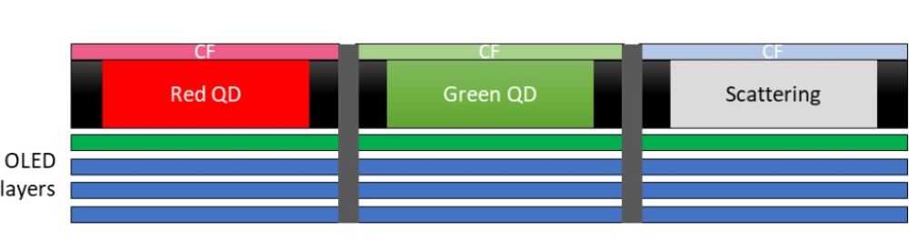
Figure 1a: Schematic of Samsung's QD-OLED architecture as reported (Ref. 1)

Figure 1b: Potential simplification with perovskite-based materials showing thinner color conversion layers, simpler OLED stack design and no color filter.
1. Thinner layers
As perovskites have significantly higher optical density than InP quantum dots, the colour conversion layer can be reduced to a few microns. This results in a faster and simpler deposition process that requires a lower volume of material. When a thinner colour conversion layer is used, the bank material holding the colour converting component can also be thinner further reducing manufacturing cost.
As the aspect ratio (height/width) of the active component shrinks, important performance benefits can be realized. The walls of each pixel are typically made of black, light absorbing material. When these walls are made shorter, there is an overall positive benefit to light output since fewer photons are lost due to absorption as illustrated in Fig. 2. For a 100 micron sub-pixel (typical for TV), it is estimated that 42% of total power is lost when the pixel wall is 15 microns high, and this value is reduced to 27% when the pixels are only 5 microns (Ref. 2). As displays push to higher and higher resolution and pixel size continues to decrease, this “aspect ratio” effect becomes even more important.
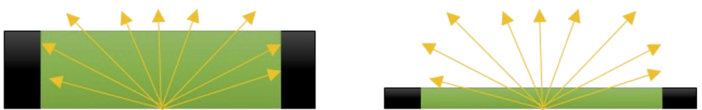
Figure 2: How thinner layers result in less photon loss
With perovskites, thinner color conversion layers will enable simpler and higher resolution fabrication of low aspect ratio structures and increase photon output (efficiency/brightness).
If deposited by inkjet printing, thinner layers will lead directly to reduced processing time. This will significantly reduce the depreciation cost per panel and yield losses.
2. Simpler OLED stack
Our eye is most sensitive to green photons, so it is important for a display to have strong green emission for increased brightness and for high dynamic range (HDR) which are both important to consumers. As green InP quantum dots do not absorb enough light to make an effective standalone colour converting layer, the current QD-OLED architecture us reported to have an additional green OLED layer. When perovskites are utilized instead of InP quantum dots, it will become possible to remove the green OLED component which significantly reduces cost and improves yield.
Additionally, performance improvements in the green and red color conversion layers will require less light to be generated by the blue OLED layers to achieve a given performance. This will further reduce cost and improve yield. The better the color conversion materials are, the faster this transition can take place.
3. Colour filter elimination
First generation colour conversion designs typically use a colour filter to block blue OLED light that leaks past the colour conversion layer unabsorbed. However, in anticipation of very high optical density and very high efficiency colour conversion solutions becoming available, the industry is already working on colour conversion architectures which don’t require a colour filter. This approach will further reduce costs and manufacturing steps. In addition, such designs are expected to be higher brightness as the photon losses associated with the colour filter are avoided.
4. Cost reduction roadmap
The benefits of manufacturing simplicity also apply to the fabrication of the perovskite materials themselves. Unlike quantum dots, there is no need to manufacture nanocrystals with sub-nanometre tolerances and the standard chemical processing used does not require high temperatures or inert atmospheres. This will enable a cost reduction roadmap that will allow perovskites to be adopted in the highest volume and most cost sensitive display applications. It will also provide interesting manufacturing alternatives, for example by enabling photolithographic processing which will greatly simplify and cost reduce deposition and patterning cost when compared to inkjet.
In conclusion, we see an enormous opportunity to apply the unique advantages of perovskites to increase both the performance and the manufacturing simplicity of colour conversion architectures. This is our development focus at Helio and we look forward to presenting our progress at major industry events during 2023 including ICDT and SID Display Week.
To find out more about Helio can help with your display design challenge, please contact us here.
References
- https://en.olednet.com/210721-2-2/
- Palomaki & Twietmeyer, 26-3, 2022 SID Symposium Digest of Technical Papers, 53 (1)